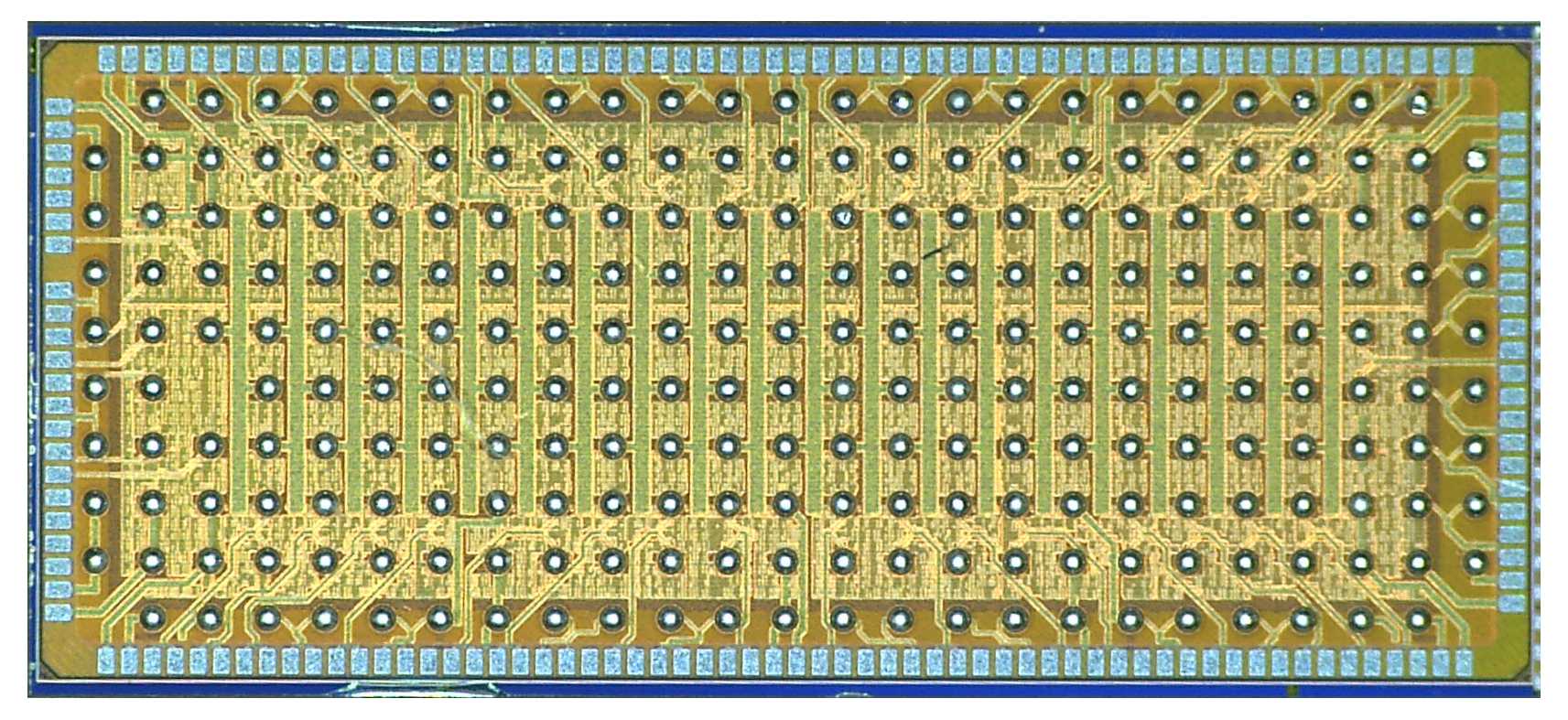
The activity of the IP2I’s Microelectronics Department is to study and design integrated circuits for particle physics, high energy, astro-particle or medical detectors. The instruments proposed by physicists generally require low-noise, low-power, multi-channel analogue circuits, but also fully digital circuits for processing and concentrating data. The environments of the circuits are generally constrained by cryogenic temperatures or high radiation levels.
The department uses the full range of microelectronic engineering techniques and collaborates closely with the departments specialising in these techniques: mechanical, instrumentation, computing and data acquisition. Its members are engineers or doctoral engineers, specialised in integrated circuit architecture and design.
The typical sequence of a project is as follows
A discussion with the scientific leaders and the establishment of the scientific and technical constraints,
Schematic design/simulation and mask design of the developed circuits,
Verification of the concept with the scientific managers,
Prototyping through multi-project foundries,
Development of test benches and quality assurance procedures,
Testing of prototypes,
Improving the performance of the concept,
Pre-production (if required), production and integration at the science experiment site.
More technical information is also available on the website of the Mi2i federation, the CNRS-NP (IN2P3) federation of microelectronics designers.
Translated with www.DeepL.com/Translator (free version)
– – PAGE UNDER CONSTRUCTION – –
The Microelectronics department is or was involved in the following projects:
- DUNE
- CMS tracker concentrateur
- R&T FASTIME
- R&T PICMIC
- R&T DoTiix
- R&T SiGe
- R&T Spider
Projets passés :
- Lojic130
- BB130
- CRONOTIC
- GAMHADRON
- HODOPIC
- ASIC Silicium
- Xtract (collaboration pole MICRHAU)
- MPTDC (circuit de Thèse)
- DSM (Circuit de Thèse)
- publications :
…
Projets Description :
CIC : Concentrateur ASIC for CMS tracker upgrade phase II

R&T FASTIME
The know-how of the Microelectronics Department of the IP2I and more generally of the IN2P3 can be summarised in a non-exhaustive way as the design and/or integration of blocks such as :
Charge and current preamplifiers,
Digital to analogue conversion circuits (DAC),
Analogue to digital conversion circuits (ADC),
Time-Delay Coders (TDC),
Phase locked loop (PLL),
Voltage Regulators (LDO),
Temperature stable voltage references (Bandgap),
Memory (flash, SRAM…),
Diodes,
Filters,
Multiplexers,
Protection circuits.
The integrated design of electronic circuits requires the mastery of design tools such as the Cadence © suite (virtuoso, spectre, pvs, innovus, genus, tempus, liberate…) to carry out simulations and the implementation of mask designs.
During the different projects and according to the needs, the designers used various technologies such as AMS, ST, IBM, TSMC, TowerJazz, in technology nodes with minimum transistor widths of 350nm, 130nm or 65nm.

Graphical representation of the specificities required of circuits for particle physics.
Translated with www.DeepL.com/Translator (free version)

