As part of a regional initiative to develop large sapphire crystals for use in extreme physics experiments and defense applications, the LMA (Advanced Materials Laboratory, a national platform of IP2I) and the mechanical engineering department of IP2I have joined forces to advance the optical polishing of these exceptional crystals.
With its extraordinary physical properties, sapphire — a crystal of aluminum oxide — is one of the most promising materials for optical applications. It features a very wide optical transmission band, from the ultraviolet to the mid-infrared range, making it ideal for use in viewports or in intense laser-based applications. Thanks to its unique characteristics — including operability at cryogenic temperatures or above 1500 °C, high thermal conductivity, and exceptional resistance to shock and abrasion — sapphire is a key material in strategic sectors such as defense, the semiconductor industry, and experiments under extreme physical conditions.
However, the very hardness of sapphire also presents a major challenge during polishing. Polishing is an essential step in the development of precision optics, as it reduces surface height errors by flattening micrometric bumps.
A New Equipment on the Doua Campus
Surface treatments of large optical components are already a specialty of the LMA (CNRS Nuclear and Particle Physics). The laboratory specializes in depositing high-performance thin films to make optical components reflective. In particular, the LMA has coated all of the most critical mirrors for gravitational wave detectors — mirrors that are considered the best in the world.
However, no expertise previously existed for the polishing step that precedes coating. To support the growing field of large sapphire optics, whose crystal growth is carried out by the Institut Lumière Matière (iLM, UCBL and CNRS Physics) also based on the Doua campus, a polishing activity has been initiated. These new developments benefit from LMA’s existing instrumentation for surface and optical property characterization, already suitable for large-size components.
As part of the CPER Recherche program (State-Region Planning Contracts), the Institut de Physique des 2 Infinis de Lyon (IP2I, UCBL and CNRS Nuclear and Particle Physics) has acquired, through State funding, a 7-axis polishing robot capable of handling substrates up to 400 mm in diameter. This equipment was delivered in fall 2024 after a year of manufacturing and six months of testing at the manufacturer Zeeko. We present here the first polishing results obtained during the first half of 2025 on sapphire samples.
A Surface Precision Down to a Few Nanometers!
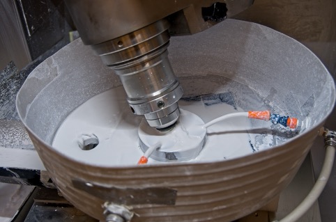
The polishing process was developed on 100 mm diameter sapphire substrates, but the technique can easily be scaled up to larger dimensions. Starting from a substrate with surface errors of 3 µm (three-thousandths of a millimeter), several polishing steps reduced these errors by a factor of 200. On the final piece, the largest bumps measured just 15 nm at the center — equivalent to about 30 sapphire molecules stacked in the crystal lattice.
“This is an excellent result, and achieved in just six months. This level of surface quality already meets 95% of optical requirements,” says Laurent Pinard, director of LMA. “It’s very promising, but we now need to focus on reducing small surface defects and polishing the substrate edges.”
The next steps will be to gradually increase the substrate size to 300 mm in diameter by 2027. This size would be compatible, for example, with a future upgrade to the Japanese gravitational wave detector KAGRA. The long-term goal is to produce the world’s finest large sapphire mirrors entirely in Lyon.
Although all developments are currently focused on sapphire, tests are planned on other materials — in particular silica glass, widely used in optics for visible and near-infrared applications.
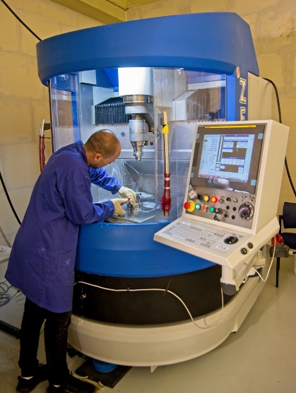
Photograph of the precision optics polishing machine recently installed at the IP2I premises on the Doua campus.
Photograph of the polishing machine for precision optics recently installed on the IP2I premises on the Doua campus.
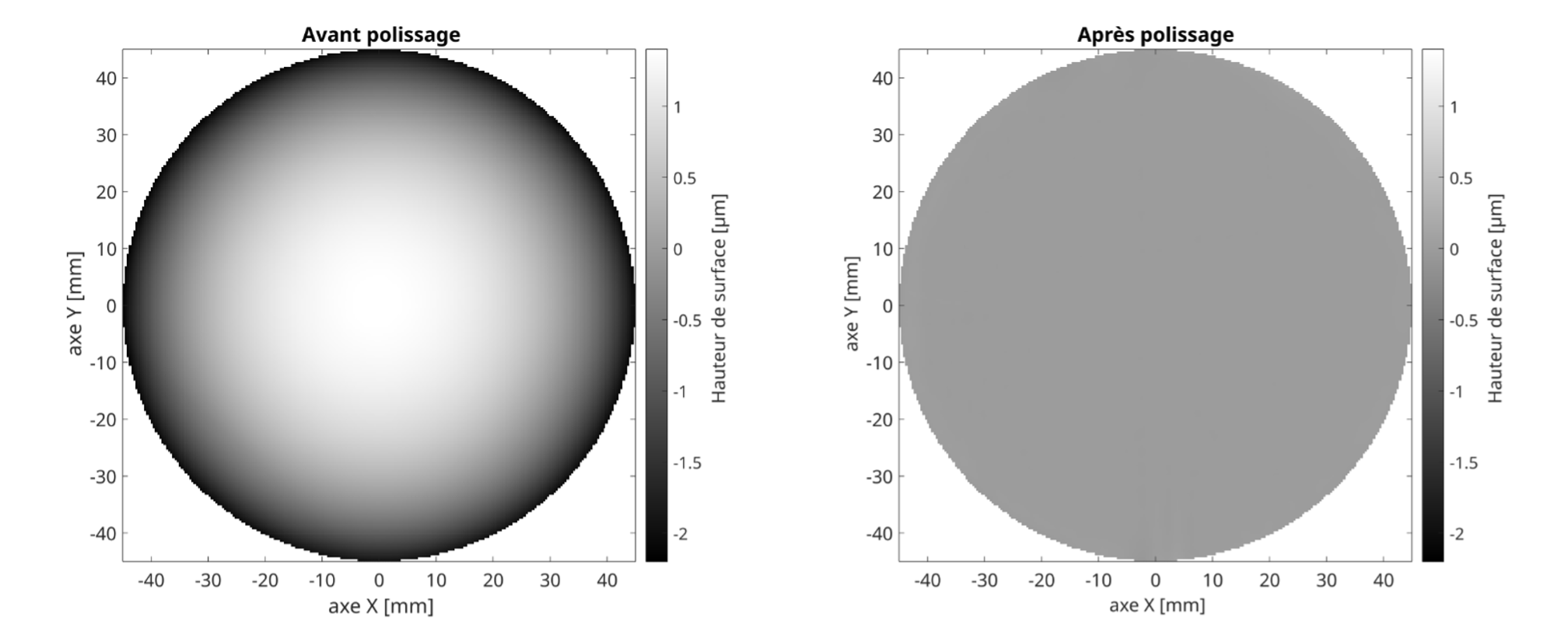
Surface height maps with monochrome scale: the same scale is used for both the pre-polishing image (left) and post-polishing image (right). The displayed area has a 90 mm diameter. Before polishing, the surface has a spherical shape; after polishing, the surface is flat.